Introduction to ARM Cortex-M & STM32 MCUs
The ARM Cortex-M is a group of 32-bit RISC ARM processor cores optimized for low-cost and energy-efficient integrated circuits. This post gives an overview about registers, memory map, interrupts, clock sources and the Cortex Microcontroller Software Interface Standard (CMSIS) library. This also shows the brief difference in STM32 MCU product lines.
Last update: 2022-05-16
Table of Content
ARM Cortex-M processors#
The ARM (Advanced RISC Machines) processors use Reduced Instruction Set Computing (RISC) architectures, and nowadays have many revisions (ARMv6, ARMv6-M, ARMv7, ARMv7-A, etc.).
ARM Cortex is a wide set of 32/64-bit core architectures, which are based on ARM architecture revisions. For example, a processor based on the Cortex-M4 core is designed on the ARMv7-M architecture.
ARM Cortex microcontrollers are divided into three main subfamilies:
- Cortex-A which stands for Application
- Cortex-R which stand for Real-Time
- Cortex-M which stands for EMbedded
Operational Modes#
The processor gives 2 Operational Modes:
- Thread mode (default)
-
- Used to execute application software
- The processor enters Thread mode when it comes out of reset
- Can be in
privilegedorunprivilegedaccess level, using bitnPRIVin theCONTROLregister
- Handler mode
-
- Used to handle exceptions. The Interrupt Program Status register
IPSRcontains the exception type number of the current Interrupt Service Routine (ISR) - The processor returns to Thread mode when it has finished exception processing
- Always in
privilegedaccess level
- Used to handle exceptions. The Interrupt Program Status register
Access Levels#
- Unprivileged
-
- Has limited access to the MSR and MRS instructions, and cannot use the CPS instruction.
- Cannot access the system timer, NVIC, or system control block.
- Might have restricted access to memory or peripherals.
- Must use the SVC instruction to make a supervisor call to transfer control to privileged software.
- Privileged (default)
-
- Can use all the instructions and has access to all resources.
- Can write to the CONTROL register to change the privilege level for software execution
Stacks#
The processor implements two stacks, the main stack and the process stack, with independent copies of the stack pointer.
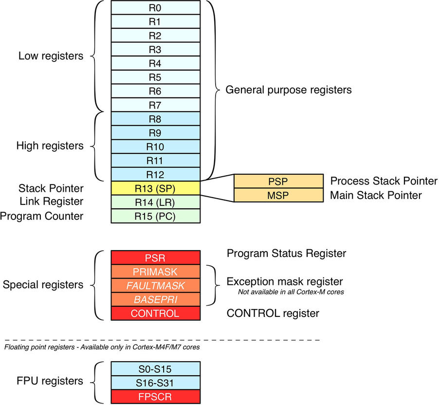
The Stack Pointer (SP) is register R13. In Thread mode, bit[1] of the CONTROL register indicates the stack pointer to use:
0: Main Stack Pointer (MSP). This is the reset value.1: Process Stack Pointer (PSP).
On reset, the processor loads the MSP with the value from address 0x00000000.
Handler mode always uses the MSP, so the processor ignores explicit writes to the active stack pointer bit of the CONTROL register when in Handler mode. The exception entry and return mechanisms update the CONTROL register.
In an OS environment, it is recommended that threads running in Thread mode use the process stack, and the kernel and exception handlers use the main stack.
Core Registers#
Like all RISC architectures, Cortex-M processors are load/store machines, which perform operations only on CPU registers except for two categories of instructions: load and store, used to transfer data between CPU registers and memory locations
-
R0~R12are general-purpose registers, and can be used as operands for ARM instructions. Some general-purpose registers, however, can be used by the compiler as registers with special functions. -
R13is the Stack Pointer (SP) register, which is also said to be banked. This means that the register content changes according to the current CPU mode (privileged or unprivileged). This function is typically used by Real Time Operating Systems (RTOS) to do context switching. -
R14is the Link Register (LR) register, which is a special-purpose register which holds the address to return to when a function call completes. This is more efficient than the more traditional scheme of storing return addresses on a call stack, sometimes called a machine stack. The linker register does not require the writes and reads of the memory containing the stack which can save a considerable percentage of execution time with repeated calls of small subroutines. -
R15is the Program Counter (PC) register, which has the address of the next instruction to be executed from memory. Usually, the PC is incremented after fetching an instruction. However, control transfer instructions can change the sequence by placing a new value in the PC register.In debugger, the
PCregister contains the address of the instruction which will be executed in next step. It is the displayed address of the instruction in the xecute stage. The actual PC value is the address of the instruction in the fetch stage (2 instruction ahead!). Read more in Load instruction example. -
Program status register (PSR) combines Application Program Status Register (APSR), Interrupt Program Status Register (IPSR), Execution Program Status Register (EPSR)
-
PRIMASKis the Priority Mask register which prevents the activation of all exceptions with configurable priority -
FAULTMASKis the Fault Mask register which prevents activation of all exceptions except for Non-Maskable Interrupt (NMI) -
CONTROLis the register that controls the stack used and the privilege level for software execution when the processor is in Thread mode and indicates whether the FPU state is active
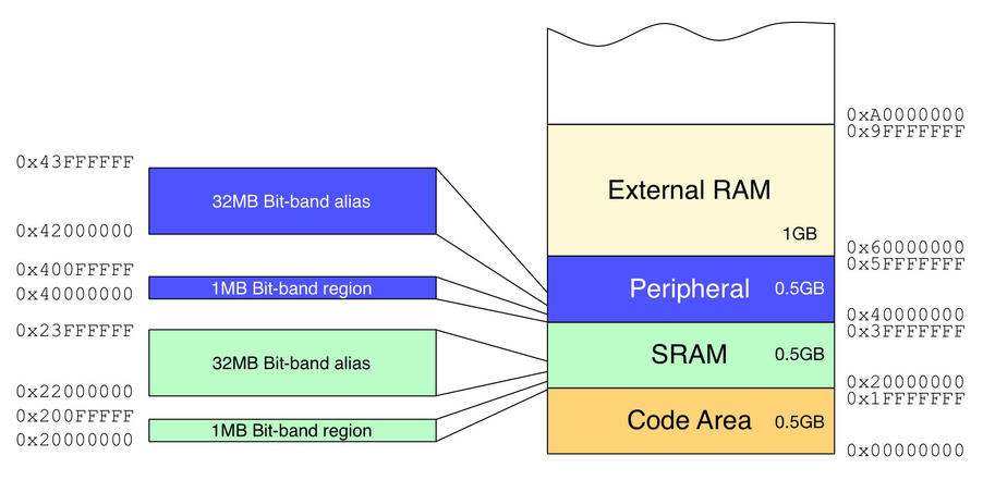
Memory Map#
ARM defines a standardized memory address space common to all Cortex-M cores, which ensures code portability among different silicon manufacturer. The address space is 4 GB wide (due to 32-bit address line), and it is organized in several subregions with different logical functionalities.
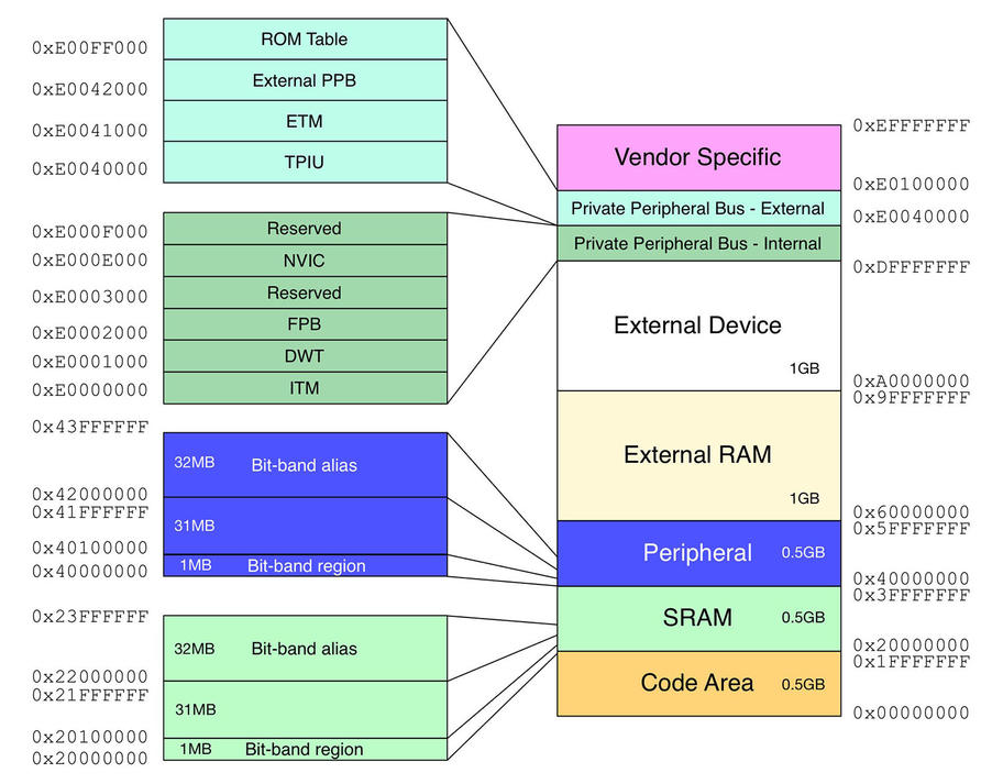
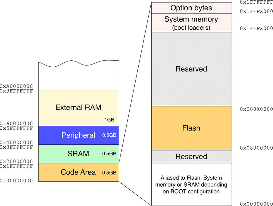
The first 512 MB are dedicated to code area:
-
All Cortex-M processors map the code area starting at address
0x00000000. This area also includes the pointer to the beginning of the stack (usually placed in SRAM) and the system interrupt vector table. -
An area starting at address
0x08000000is bound to the internal MCU flash memory, and it is the area where program code resides. With a specific boot configuration, this area is also aliased from address0x00000000. This means that it is perfectly possible to refer to the content of the flash memory both starting at address0x08000000and0x00000000. -
System Memory is a ROM region filled with official pre-programmed Bootloader which can be used to load code from several peripherals, including USARTs, USB and CAN bus.
-
Option Bytes region contains a series of bit flags which can be used to configure several aspects of the MCU (such as flash read protection, hardware watchdog, boot mode and so on) and are related to a specific microcontroller.
Next 512 MB is mapped to Internal SRAM:
-
It starts at address
0x20000000and can potentially extend to0x3FFFFFFF. -
This area also can be aliased to the start-up address at
0x00000000to execute code in internal RAM.
The left space is for peripherals and other stuff:
- Other memory regions are mapped to external RAM, peripherals and the internal core registers. All Cortex processor registers are at fixed locations for all Cortex-based microcontrollers. This allows code to be more easily ported between different core variants and indeed other vendors’ Cortex-based microcontrollers.
Bit-Banding#
In embedded applications, it is quite common to work with a single bit of a word using bit-masking. For example:
uint8_t flags = 0;
flags |= 0x4; // set the 4-th bit
generates assembly code :
0x0a: 79fb ldrb r3, [r7, #7]
0x0c: f043 0304 orr.w r3, r3, #4
0x10: 71fb strb r3, [r7, #7]
Such a simple operation requires three assembly instructions (fetch, modify, save). This leads to a problem if an interruption happens between processing bit mask.
Bit-banding is the ability to map each bit of a given area of memory to a whole word in the aliased bit-banding memory region, allowing atomic access to such bit.
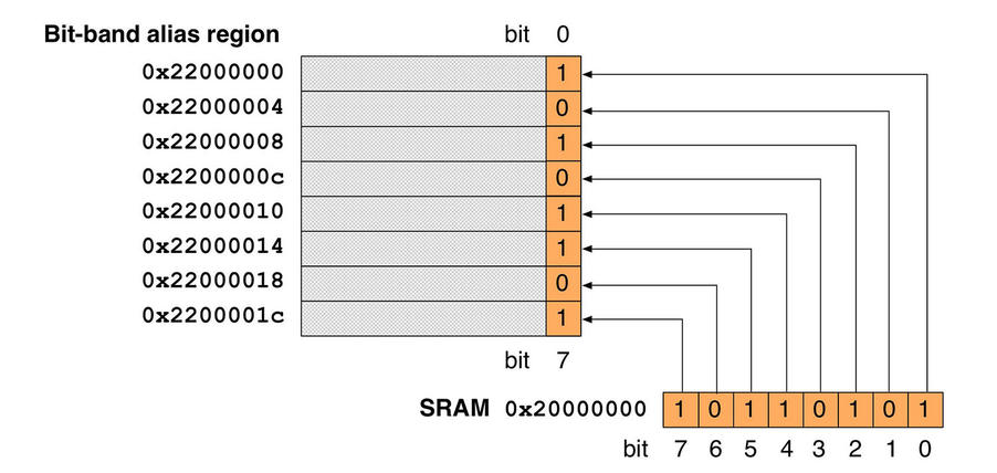
ARM defines two bit-band regions for Cortex-M based MCUs, each one is 1 MB wide and mapped to a 32 Mbit bit-band alias region.
-
The first one starts at
0x20000000and ends at0x200FFFFF, and it is aliased from0x22000000to0x23FFFFFF. It is dedicated to the bit access of SRAM memory locations. -
Another bit-banding region starts at
0x40000000and ends at0x400FFFFF, which is dedicated to the memory mapping of peripherals, from0x42000000to0x43FFFFFF.
Define two macros in C that allow to easily compute bit-band alias addresses:
/* MEMORY BIT-BANDING */
// Define base address of bit-band
#define BITBAND_SRAM_BASE 0x20000000
// Define base address of alias band
#define ALIAS_SRAM_BASE 0x22000000
// Convert SRAM address to alias region
#define BITBAND_SRAM(a,b) ((ALIAS_SRAM_BASE + ((uint32_t)&(a)-BITBAND_SRAM_BASE)*32 + (b*4)))

/* PERIPHERAL BIT-BANDING */
// Define base address of peripheral bit-band
#define BITBAND_PERI_BASE 0x40000000
// Define base address of peripheral alias band
#define ALIAS_PERI_BASE 0x42000000
// Convert PERI address to alias region
#define BITBAND_PERI(a,b) ((ALIAS_PERI_BASE + ((uint32_t)a-BITBAND_PERI_BASE)*32 + (b*4)))
Example that quickly modifies the state of PIN5 of the GPIOA port as follows:
#define GPIOA_PERH_ADDR 0x40020000
#define ODR_ADDR_OFF 0x14

uint32_t *GPIOA_ODR = GPIOA_PERH_ADDR + ODR_ADDR_OFF
uint32_t *GPIOA_PIN5 = BITBAND_PERI(GPIOA_ODR, 5);

*GPIOA_PIN5 = 0x1; // Turns GPIO HIGH
Thumb Instruction Set#
ARM Cortex-M processors provide a 32-bit instruction set, not only allows for a rich set of instructions, but also guarantees the best performance. However, memory footprint of the firmware has bigger cost. To address such issues, ARM introduced the Thumb 16-bit instruction set which is transparently expanded to full 32-bit ARM instructions in real time, without performance loss. Afterwards, ARM introduced the Thumb-2 instruction set, which is a mix of 16 and 32-bit instruction sets in one operation state.
The T bit of EPS Register
The Execution Program Status Register (EPSR) as a T bit to indicate Thumb state.
If T but is 1, next instruction is Thumb ISA.
If T but is 0, next instruction is ARM ISA.
The Cortex-M4 processor only supports execution of instructions in Thumb state. Hence, the T bit must be always 1.
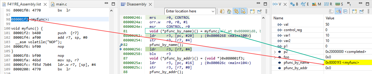
The LSB (bit 0) of the Program Counter (PC) register is loaded to that T bit when the PC register is written. Therefore, any address that is put into PC register must be odd. This is usually taken care by the compiler. In case you call a function by an address manually, you have to take care the LSB bit of the address yourself.
void myfunc() {
  __asm volatile("nop");
}
int main() {
    // at 0x080001d8, but compiler will assign value 0x080001d9
    void (*pfunc_by_name)() = myfunc;
    pfunc_by_name();

    // manual load an address shoule be careful
    // use 0x080001d8 will cause Usage Fault Exception: Invalid State
    void (*pfunc_by_addr)() = (void *)0x080001d9;
    pfunc_by_addr();
}
Instruction Pipeline#
Before an instruction is executed, the CPU has to fetch it from memory and decode it. So, it has 3 stages to complete an instruction. Modern CPUs introduce a way to parallelize these operations in order to increase their instructions’ throughput. The basic instruction cycle is broken up into a series of steps, as if the instructions traveled along a pipeline.

When dealing with pipelines, branching is an issue to be addressed. When branching causes the invalidation of pipeline streams, the last two instructions which have been loaded into the pipeline will be discarded.
Memory Alignment#
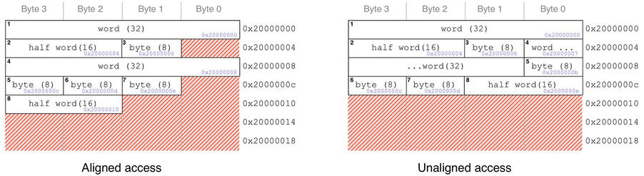
ARM based CPUs are traditionally capable of accessing byte (8-bit), half word (16-bit) and word (32-bit) signed and unsigned variables, without increasing the number of assembly instructions as it happens on 8-bit MCU architectures which reads byte by byte. Aligned memory access causes a waste of memory locations.
Interrupts and Exceptions#
Interrupts and exceptions are asynchronous events that alter the program flow. When an exception or an interrupt occurs, the CPU suspends the execution of the current task, saves its context (that is, its stack pointer) and starts the execution of a routine designed to handle the interrupting event. This routine is called Exception Handler in case of exceptions and Interrupt Service Routine (ISR) in case of an interrupt. After the exception or interrupt has been handled, the CPU resumes the previous execution flow, and the previous task can continue its execution. In the ARM architecture, interrupts are one type of exception.
-
Interrupts are usually generated from on-chip peripherals (e.g., a timer) or external inputs (e.g. a tactile switch connected to a GPIO), and in some cases they can be triggered by software.
-
Exceptions are, instead, related to software execution, and the CPU itself can be a source of exceptions.
Each exception (and hence interrupt) has a number which uniquely identifies it. Cortex-M cores has pre-defined exception table which contains the addresses of function to handle those exceptions.
| Number | Exception Type | Priority | Function |
|---|---|---|---|
| 1 | Reset | -3 | Reset |
| 2 | NMI | -2 | Non-Maskable Interrupt |
| 3 | Hard Fault | -1 | All faults that hang the processor |
| 4 | Memory Fault | Configurable | Memory issue |
| 5 | Bus Fault | Configurable | Data bus issue |
| 6 | Usage Fault | Configurable | Data bus issue |
| 7 ~ 10 | Reserved | — | Reserved |
| 11 | SVCall | Configurable | System service call (SVC instruction) |
| 12 | Debug | Configurable | Debug monitor (via SWD) |
| 13 | Reserved | — | Reserved |
| 14 | PendSV | Configurable | Pending request for System Service call |
| 15 | SysTick | Configurable | System Timer |
| 16 ~ 240 | IRQ | Configurable | Interrupt Request |
System Timer#
Cortex-M based processors can optionally provide a System Timer, also known as SysTick which is a 24-bit down-counting timer used to provide a system tick for Real Time Operating Systems (RTOS). It is used to generate periodic interrupts to scheduled tasks, or measure delay. When the timer reach zero, it fires an interrupt number 15, as seen in the Interrupt Table above.
Power Mode#
Cortex-M processors provide several levels of power management which can be set via System Control Register (SCR).
- Run mode: full clock speed, all using peripherals are activated
- Sleep mode: reduced clock speed, some peripherals are suspended
- Deep sleep mode: clock is stopped, need external event to wake-up
CMSIS for SW development#
Cortex Microcontroller Software Interface Standard (CMSIS) is a vendor-independent hardware abstraction layer for the Cortex-M processor series and specifies debugger interfaces. The CMSIS consists of the following components:
- CMSIS-CORE: API for the Cortex-M processor core and peripherals
- CMSIS-Driver: defines generic peripheral driver interfaces for middleware making them reusable across supported devices
- CMSIS-DSP: API for process signal and data such as fixed-point, single precision floating-point
- CMSIS-RTOS API: Common API for Real-Time Operating Systems
- CMSIS-Pack: a set of collections which includes source, header, library files, documentation, flash programming algorithms, source code templates and example projects
- CMSIS-SVD: System View Description for Peripherals
- CMSIS-DAP: Debug Access Port
Cortex-M comparison#
A table excerpted from ARM website.
| Feature | Cortex-M0 | Cortex-M0+ | Cortex-M3 | Cortex-M4 | Cortex-M33 | Cortex-M7 |
|---|---|---|---|---|---|---|
| ISA | Armv6-M | Armv6-M | Armv7-M | Armv7-M | Armv8-M Mainline | Armv7-M |
| Thumb, Thumb-2 | ||||||
| Pipeline stages | 3 | 2 | 3 | 3 | 3 | 6 |
| Memory Protection Unit | No | Yes | Yes | Yes | Yes | Yes |
| Maximum MPU regions | 0 | 8 | 8 | 8 | 16 | 16 |
| Trace (ETM or MTB) |
No | MTB | ETMv3 | ETMv3 | MTB and/or ETMv4 | ETMv4 |
| DSP | No | No | No | Yes | Yes | Yes |
| Floating point hardware | No | No | No | Yes | Yes | Yes |
| Bus protocol | AHB Lite | AHB Lite | AHB Lite, APB | AHB Lite, APB | AHB5 | AXI4, AHB Lite, APB, TCM |
| Maximum # external interrupts | 32 | 32 | 240 | 240 | 480 | 240 |
| CMSIS Support | Yes | |||||
STM32 Microcontrollers#
STM32 is a broad range of ARM Cortex-M microcontrollers divided in nine subfamilies. Internally, each microcontroller consists of the processor core, static RAM, flash memory, debugging interface, and various peripherals.
Here are advantages of using STM32 MCUs:
-
Cortex-M based MCUs have a large community, supported by free tool-chain, and is written in many shared knowledge articles
-
The Pin-to-Pin compatibility for most of STM32 MCUs helps to change the MCU while keeping pin assignments
-
Almost pins are 5V tolerant, that means it can interface with other devices which do not use 3.3V without using level shifter
-
Cheap is an advantage of using STM32 MCUs with ARM based processors and supported RTOS
-
Integrated bootloader is shipped with internal ROM which allows to reprogram the internal flash memory using some communication peripherals
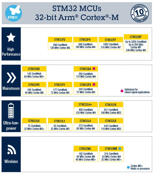
STM32 MCUs comparison
| Type | Family | Core | Max Frequency | Flash |
|---|---|---|---|---|
| High Performance | STM32H7 | Cortex-M7 / Cortex -M4 | 480 MHz / 240 MHz | 1 to 2 MB |
| STM32F7 | Cortex-M7 | 216 MHz | 256 KB to 2 MB | |
| STM32F4 | Cortex-M4 | 180 MHz | 64 KB to 2 MB | |
| STM32F2 | Cortex-M3 | 120 MHz | 128 KB to 1 MB | |
| Mainstream | STM32G4 | Cortex-M4 | 170 MHz | 32 to 512 KB |
| STM32F3 | Cortex-M4 | 72 MHz | 16 to 512 KB | |
| STM32F1 | Cortex-M3 | 72 MHz | 16 KB to 1 MB | |
| STM32G0 | Cortex-M0+ | 64 MHz | 16 to 512 KB | |
| STM32F0 | Cortex-M0 | 48 MHz | 16 to 256 KB | |
| Ultra-low-power | STM32L5 | Cortex-M33 | 110 MHz | 256 to 512 KB |
| STM32L4+ | Cortex-M4 | 120 MHz | 512 KB to 2 MB | |
| STM32L4 | Cortex-M4 | 80 MHz | 64 KB to 1 MB | |
| STM32L1 | Cortex-M3 | 32 MHz | 32 to 512 KB | |
| STM32L0 | Cortex-M0+ | 32 MHz | 8 to 192 KB | |
| Wireless | STM32WB | Cortex-M4 / Cortex-M0+ | 64 MHz / 32 MHz | 256 KB to 1 MB |
| STM32WL | Cortex-M4 | 48 MHz | 64 KB to 256 KB |